
Dr. Jinesh K B
Area of Research
Education
- Ph.D (Physics): Leiden University, The Netherlands
- Ph.D (Electrical Engineering): Twente University of Technology, The Netherlands
- M.Sc. (Physics): Cochin University of Science and Technology (CUSAT), Cochin, India.
- B.Sc (Physics): Mahatma Gandhi University, Kottayam, Kerala, India.
H-index (as on 2025 June): 27
Total citation (as on 2025 June): 2723
Faculty Development Programme Lectures:
- Scanning Electron Microscopy: Mahatma Gandhi University, March 2024
- Scanning Probe Microscopes: Central Laboratory for Instrumentation and Facilitation (CLIF), Kerala University (October 2022)
- Scanning Tunneling Microscopy and Spectroscopy, Bharathiar University (January 2020)
- Scanning Probe Microscopy, University of Kerala (November 2019)
- Intellectual Property Rights and Patents, University of Kerala, Karyavattom Campus (2017 March)
- Nanomaterials: application perspectives, University of Kerala, Karyavattom Campus (2016 Nov.)
- Graphene: Department of Physics, University of Kerala, Karyavattom campus (2015 Dec.)
- Introduction to Nanoelectronics: Amal Jyothi College of Engineering (2015 April).
- The revolutions in the Electronic Memory: TKM College, Kollam (2015 March).
- Technology Roadmaps: University of Kerala, Karyavattom campus (2014 Nov.).
- Nanotechnology Roadmaps: Department of Physics, University of Kerala, Karyavattom campus (2014 Nov.).
Ph.D. Programs:
Completed:
- Resistive RAM and Neuromorphic Systems: Role of Ions and Interface States: Ph.D. work of Dr. Preetam Hazra (Ph.D. awarded: 2020 October. (Currently at IIT Mumbai)
- Two-Dimensional materials and their derivatives for Neuromorphic Memory Applications: Dr. Anna Thomas (2022)
- Pulsed Laser Deposited BFO Thin Films for Neuromorphic Memory Applications: Mr. Dayal. G (2024 September 4)
Ongoing:
- Pavlovian Conditioning in Neuromorphic Systems: Mr. Viswajit. R.S. (2021-)
- Atomic Layer Deposition and Applications: Mr. Jyothish Raj (2021-)
- Carbon materials for Space Applications: Ms. Debashree Das (2021-)
- Inelastic Electron Tunneling Spectroscopy using Scanning Tunneling Microscope: Ms. Archana Thomas (2022-)
- Optical Neuromorphic systems: Mr. Abhijith Anand (2022-)
- Magnetron-Sputtered metal oxides for neuro-logic applications: Ms. Vaishnavi (2022-)
- Ferroelectric Tunnel Junctions for Neuromorphic Applications: Sanchari Pal (2022-)
Master's Projects
2024
- Atomic Layer Deposition of ZnO: S. Shanmughapriya, Amritha Vishwavidyalayam, Kollam
- Pulsed Laser Deposition of BaSrTiOx for high-k applications: Vani Prasad, Amritha Vishwavidyalayam, Kollam
2023
- Determination of the process window of Al2O3 deposition in Thermal Al2O3: Mr. Anuvind K.K., SN College, Kollam.
- Pulsed Laser Deposited MoS2 for neuromorphic applications: Ms. Joja. J.M. (Kerala University)
- Role of Schottky barrier on the neuromorphic properties of BiFeO3 artificial Synapses: (Mr. Easwaran, Kerala University)
2022
- Tunable resistive memory using nanoparticle-incorporated active layers: Ms. Bismiya Fasni (IISER Tirupati)
- CuPc-based optical detectors: Smrithi S (Kerala University)
- Pulsed-Laser-Deposited HfO2 for memory applications: Meenu Jayan (Kerala University)
2019
- Crossbar ReRAM Memory and sneaking currents; Harsh Kadian (IIT Ropar)
- Lithium doped ZnO by spray pyrolysis; Anaswara Ramdas (Govt. College, Madappally)
- Metal quantum dots by pulsed laser ablation; Greeshma. G (Mercy College, Palakkad)
- Simulations of multi-layer memory devices; Anu. K.M. (Mercy College, Palakkad)
- STM studies of MoS2 on graphite; Ajay B.U. (M.G. College, Trivandrum)
- Synthesis of MoS2 quantum dots and their characterization; Megha. P.K. (M.G. College, Trivandrum)
- Optoelectronic properties of MoS2 quantum dots; Shahna Hakkim (M.G. College, Trivandrum)
- Pulsed laser deposition of Fe:ZnO; Vishnu G Nath (Govt. College, Calicut)
- Optical memory using CuPC thin films; Kiran Jose (Christ College, Bangalore)
- Synthesis of Nanodiamonds and their coatings; Aruja Jose (Marthoma College, Thiruvalla)
- Operational statistics of Crossbar memory arrays; Sachin Jose and Joice Thomas (K.E. College, Mannanam)
- Manganese doped ZnO for optoelectronics; Kanzul Karim (Vellore Institute of Technology, Chennai)
- Pulsed laser deposition of ZnO and doped ZnO; Anitta Jose, Anjana Roy (CUSAT, Cochin)
2018
- Optoelectronic properties of CuPc/Alq3 p-n junctions and applications in Photosensing and Light Emitting Diodes; Ms. Afiya. M. Raj, Kerala University (M.Tech Project).
- Liquid Phase Pulsed Laser Ablation of graphene and its optoelectronic applications; Ms. Parvathy S, Kerala University (M.Tech Project).
- Resistive RAM devices using nanoparticle embedded PMMA thin films; Ms. Ayswarya Suresh, Mar Thoma College, Ayur (M.Sc Project).
- Resistive Random Access Memory (ReRAM) devices: Ms. Asmita Jash (M.Tech. Project, IIST).
- Mixed Halide Perovskite Solar Cells: Towards Iodine Free High-Efficiency Solar Cells: Ms. Jayita Dutta (M.Tech. SST Project).
- Bandgap statistics of single-layer MoS2 using Scanning Tunneling Microscope; Akhil Mohanan, Kannoor University (M.Sc. Projects).
- Spectroscopy of MoS2 Quantum Dots: Nayana. S, St Xaviers College, Thumpa (M.Sc. Project).
- Resistive memory behavior in ZnO p-n junctions: Meenu. P. NSS College, Ottapalam (M.Sc. Project).
- Resistive memory using Graphene-intercalated PMMA layers; Beena. K. NSS College, Ottapalam (M.Sc. Project).
- Nano-lithography using Scanning Tunneling Microscope; Hyiday Dath (MS Dual Degree Mini Project).
- Modeling of MoS2 Thin-Film Transistors; Nandakishor. M. (MS Dual Degree Mini project).
2017
- Optical sensors using reduced graphene oxide (cont.): Ms. Greeshma P.S. (M.Tech project, University of Kerala)
- Photoconductivity of MoS2 Thin Films and Quantum Dots: Ms. Lekshmi P.R. (M.Tech project, University of Kerala)
- Metal electrodes for ReRAM Technology, Mr. Jeevan Philip (M.Tech project, IIST).
- Resistive switching in MoS2 quantum dots; Akash Ganguly (B.Tech. Engineering Physics, IIST) (Currently at ISRO)
- MoS2 Thin film transistors, Jay Bhutt (B.Tech. Engineering Physics, IIST) (Currently at ISRO)
- ReRAM devices using Carbon dots, Sandeep Kumar (B.Tech Avionics, IIST) (Currently at ISRO)
- Flexible organic memory devices: Rajat Kumar (B.Tech Avionics, IIST) (Currently at ISRO)
- Modeling of IR Bolometers for thermal imaging: Mr. Dinesh Jangid (B.Tech. Avionics, IIST) (Currently at ISRO)
2016
- Effect of molecular weight on the resistive switching of PMMA; Ms. Jeena Varghese, M.Sc project (Univ. College, Trivandrum) (Currently doing PhD at Adam Mickiewicz University Poznan, Poland)
- Optical detectors using reduced Graphene oxide: M.Tech project Mr. Rajkrishnan (Kerala University),
- Thin film transistors using graphene derivatives; Somnath Chakraborty, M.Tech project.(currently doing PhD at IIT Mumbai).
- CdTe-based Thin film Solar cells: Maheswari S, M.Tech Project (currently doing PhD at NUS, Singapore).
- ZnO-based thin film transistors using spray pyrolysis: Joel Zacharias, M.Tech Project. (Currently PhD student, IIST)
- Switching mechanisms of graphene oxide: Silpasree S.J., Amrita Vishwa Vidyapeetham, Kollam, M.Sc project (currently doing PhD at Amrita Institute of Nanosciences).
- Bandgap statistics of graphene oxide reduced by Nd-YAG laser: Harikrishnan. K.S. MAMO College, Mukkam, M.Sc project.
- Resistive switching in Ag/PMMA/FTO devices as a functionof PMMA Thickness: Aleena Johnson and Keerthana K.K., Devamatha College, Kottayam, M.Sc Project
- Laser-induced reduction of Graphene oxide: Athira Jose, N.S.S. College, Palakkad, M.Sc project.
- Preparation and characterization of Mn-doped ZnO: Nandan Babu, NIT Calicut, M.Sc Project. ( Currently doing PhD at Adam Mickiewicz University Poznan, Poland).
2015
- Resistive Random Access Memory (ReRAM) devices based on Inorganic, organic and hybrid materials; Ms. Shivani Agarwal, M.Tech project (currently doing PhD at IIT Mumbai).
- Plasmonic transistors with reduced graphene oxide: Ms. Renuka Devi, M.Tech project (currently doing PhD at Italian Institute of Technology).
- Design of a novel transistor architecture for the modern sub-14nm ULSI era: M.Tech project by Mr. Uttam Kumar (currently at IIT Kharagpur).
Completed Internships:
- Physically Unclonable Functions using PMMA-graphene hybrid devices: S.R. Nidhin, Central University of Tamil Nadu (2016).
- Laser-induced synthesis of carbon dots from graphene oxide: R. Akshay Raj, IISER Kolkata (2016)
- CuZnAlS2 for resistive memory applications: P. Alan, IISER Bhopal (2016)
- Cu-doped ZnO for resistive RAM applications: Ms. P.V. Sruthibhai, IISER Bhopal (2015).
- Thin-film transistors using spray-coated Cu:ZnO thin films: Mr. K. Somesh, IISER Bhopal (2015).
- Resistive switching in polymethyl methacrylate (PMMA) thin films: Mr. Jimmy Mangalam, Amity Institute of Nanotechnology, Noida UP (2015).
- Synthesis and characterization of Mn-doped ZnO nanocones; C.G. Lakshmi, IISER Trivandrum (2014).
- Synthesis of TiO2 nanoparticles for electrochemical water splitting: Maneesha Ismail, IISER Kolkata (2014).
Funded Project
Completed Projects:
1. Electronic manipulation of surface plasmon polaritons on graphene: IIST Fast-Track project, (2014-2016): 10 Lakhs
2. Surface Engineering Techniques for Improving the Life Performance of Ball Bearing Systems of ISRO Spacecraft Systems: Funded by ISRO Inertial Systems Unit, ISRO (IISU, 49.6 Lakhs)
3. Development of Surface Discharge Sparkplugs: Funded by Liquid Propulsion Systems Center, ISRO (LPSC, 23.64 Lakhs).
Ongoing Projects
- Development of an Atomic Layer Deposition System: Project funded by Department of Science and Technology (DST), 2021 (1.22 Crores)
- Development Laser Ignition Systems: Funded by Liquid Propulsion Systems Center, ISRO (LPSC; 31.14 Lakhs)
- High-Q Dielectric Thin Films with Tunability in Microwave Frequencies for Space Applications : Funded by Vikram Sarabhai Space Center, ISRO (VSSC, 40.64 Lakhs)
- Development of Yttrium Iron garnet (YIG) thin films for Space Applications and Deielectric Test setup for ceramics at high Electric fields and Temperatures: Funded by Vikram Sarabhai Space Center, ISRO (VSSC, 9.64 Lakhs).
- Design and construction of MEMS-based portable Seismocardiogram for on-board Cardiac health monitoring of Astronauts: Funded by Laboratory for Electro-Optics Systems, ISRO (LEOS, 11.22 Lakhs)
Teaching Interest
1. Semiconductor Physics
2. Device Physics and Nanoelectronics
3. Solid State Physics
4. Process Technology
Area of Interest
- Future memory technology for data storage, neuromorphic devices for Artificial Intelligence applications, applications of Resistive Random Access Memory (ReRAM or RRAM) for neural networks, cryptography and quantum computation and information processing.
- Thin film transistors and future electronic materials for fast communication, display applications.
- Process technology and integration: nanoelectronic devices and their charge transport mechanisms.
- Atomic Layer Deposition: instrumentation and techniques, new materials and recepies, applications in micro and nanoelectronics.
Patents:
- US20120151997: Method of making an electrically conductive structure, method of making a gas sensor, gas sensor obtained with the method and use of the gas sensor for sensing a gas; K.B. Jinesh, M. Crego-Calama, S. Brongersma (2012).
- US2011263036: Amorphous thin film for sensing; M Blauw, V.A. Dam Thi, K.B. Jinesh (2012).
- US2011163088: Token comprising improved physical unclonable function; K.B. Jinesh, W.F.A Besling (2011).
- US2011147891: Capacitor and a method of manufacturing the same; Y. Furukawa, K.B. Jinesh, J.H. Klootwijk, F. Pasveer (2011).
- US2011148529: Radio frequency amplifier with effective decoupling; W.F.A. Besling, W.T. Bakker, Y. Lamy, F. Roozeboom, K.B. Jinesh (2011).
- US2011128727: Integrated Seebek device; K.B. Jinesh, J.H. Klootwijk (2011).
- US2011101471: Method of forming a nanocluster-comprising dielectric layer and device comprising such layer; K.B. Jinesh, W.F.A Besling, J.H. Klootwijk, R.A.M. Wolters, F. Roozeboom. (2011)
- WO2010103452: Low-frequency filter comprising Maxwell-Wagner stack; K.B. Jinesh, W.F.A. Besling (2010)
- WO2010038216: Phase-change memory cells and fabrication thereof; K.B. Jinesh, R.A.M. Wolters, M.A. Zandt (2010)
- WO2010018490: A photovoltaic cell and method of manufacturing the same; Y. Furukawa, F. Pasveer, J.H. Klootwijk, K.B. Jinesh (2010).
- WO2009153728: Through-wafer via filling method; K.B. Jinesh, Y. Lamy (2009).
- WO2009150600: Enhanced surface area structure; K.B. Jinesh, F. Roozeboom, J.H. Klootwijk, W. Dekkers (2009).
Invited talks: (International conferences
- Brain-inspired memory technologies: Functional Materials for Energy, Environment and Biomedical Applications (FARAON); Madurai Kamaraj University, (4th February 2022)
- Future Memory technologies: role of high bandgap semiconductors: International Seminar on Large Band Gap Semiconductors, IISER Trivandrum, India (23 January 2019)
- Atomic layer deposition: from materials to applications: Institute of Smart Structures and Systems 2017 Conference, IISc, Bangalore, India (July 2017)
- Material and Scaling Challenges of Resistive Randon Access Memory Technology; Int. Nat. Conference on Materials for Power Engineering, M.G. University, kerala, India (Dec. 2015).
- Atomic-scale friction: effects of Capillary condensation; IBM, Zurich, Switzerland (2006 August).
- Ice-formation at room-temperature due to nano-confinements: Micro and Nanotribology international conference, Warsaw, Poland (September 2005).
Atomic layer deposition: Technology towards More than Moore: International conference on Advanced Materials and Applications, Alphonsa College, Palai, Kerala, India
Invited talks: (National conferences/seminars)
- Physics for Next-Generation Engineering: Induction Program at Lourdes Matha College, Kattakkada, (July 2023)
- Nano-materials for Artificial Intelligence; National Conference on Nano Materials; Cochin University of Science and Technology (January 2020)
- Material Perspectives of Next Generation Memory and Computation; St. Thomas College, Ranni (December 2019)
- Electronic Memory technology: ReRAMs; Invited lecture at Crescent University of Science and Technology, Chennai (September 2019)
- Physics of artificial intelligence: Government Engineering College, Induction program (August 2019)
- Evolution of microscopes: seing and playing with atoms: National Science Day Lecture, Rajiv Gandhi Center for Biotechnology (RGCB), Thiruvananthapuram (28 February 2019)
- Material Challenges of Future memory tachnology; National Conference on Advanced Functional Materials, Hindu College, Nagarcoil (25 February 2018)
- Where Physics meets Artificial Intelligence; National Seminar on Advances in Theoretical and Experimental Physics, Govt. Women's College, Trivandrum (26 October 2018)
- The physics of future memory technologies, National Seminar on Functional Materials, Assumption College, Changanassery (28 September 2018)
- Intellectual Property Rights and Patents; Kerala University (October 2018)
- Seeing and playing with Atoms, National Seminar on Foundations of Physics, Government College, Nedumangad, January 12, 2018.
- Scanning Tunneling Microscopy and Spectroscopy; National Seminar on Quantum mechanics, Assumption College, Changanacherry (December 2017)
- Quantum Tunneling in Technology:National Seminar on Quantum mechanics, Assumption College, Changanacherry (December 2017)
- Graphene-based technologies: An overview: National Seminar on Advanced Materials, Mar Ivanios College, Thiruvananthapuram (December 2017)
- Graphene for Optoelectronics applications: National Seminar on Materials for electronic and Optoelectronic Applications, CMS College, (November 2017)
- Intellectual Property Rights and Patents; Kerala University (October 2017)
- From Nano to Nano; World Space Week, LPSC Trivandrum (October 2017)
- Technology Roadmaps, Government Arts College, Trivandrum (February 2017)
- It's all about Nanotechnology; IIST at School Program, Thalassery, Kannur, Kerala (November 2016)
- Optical properties of Reduced Garphene Oxide devices, National Seminar on Solar Photochemistry : Fundamentals & Applications, Fatima Mata National College, Kollam (January 2016)
- Scaling down the transistors: Phyics and Technology, National Seminar or Nanomaterials for Energy Applications, S.N. College, Punalur (January 2016).
- Opto-electronics with Reduced Graphene Oxide; National Seminar on Optoelectronics, Kerala University, Trivandrum (2015 Dec.)
- Materials for ReRAM Technology; National Seminar on Advanced Materials, St. Pauls College, Cochin (2015 Dec.)
- Resistive Random Access Memory Technology; Nat. Conference on Advanced Materials, Deamatha College, Kottayam (2015 Dec.)
- Graphene: Department of Physics, University of Kerala, Karyavattom campus; FDP (2015 Dec.)
- ReRAM: the future of electronic memory technology: St.Stephens College, Pathanapuram, Kollam (2015 November)
- Introduction to nanoelectronics; Amal Jyothi College of Engineering, FDP (2015 April)
- The revolutions in the Electronic Memory: Advances in Nanotechnology (FDP), TKM College of Engineering, Kollam (2015 March).
- Trends in Nanotechnology Research: National Seminar on Nanoscience and Nanotechnology, SN College, Varkkala (2015 March)
- Living in the Quantum World; Nantional Seminar on Nanotechnology, SN College Chempazhanthi (2015 March)
- Quantum Alzheimer's: the future of the Electronic Memory: University College, Kerala, Trivandrum (2015 January)
- The Trends and Evolutions in Technology: Vins college of Engineering, Nagarcoil (2015 February).
- Evolutions in Nanotechnology: Bohr Model workshop, St. Thomas College, Palai, Kerala (2014 December)
- Nanotechnology roadmaps, Kerala University FDP (2014 November)
- Technology Roadmaps: Kerala University FDP (2014 November)
- Beyond Moore: Advances in miniaturization technology; Nanoscience Conference, Central University of Kerala (2014 October)
- Nano-plasmonics: National Science Day Seminar, Department of Photonics, Cochin University of Science and Technology, Kerala, India (2014 February)
- From Bohr to Bohr: evolutions in nanotechnology: Seminar on 100th Anniversary of Bohr atom Model, Physics Dept., CUSAT (2014 February)
- Is there enough room at the bottom? Kerala Breakthrough Science Society; Priyadarshini Planetarium (2014 January)
- Nanotechnology – basics and perspectives: Cochin University of Science and Technology, India (August 2004).
Atomic layer deposition– Special seminar, Cochin University of Science and Technology (CUSAT) India, (December 2010)
Other Talks:
- Ice-formation at room temperature in atomic-scale friction: Nanotribology conference, Antalya, Turkey (September 2006).
- Capillary condensation in atomic friction: Physical Preview Lunch meeting, Leiden, The Netherlands (January, 2006).
- Capillary Condensation in atomic friction: FOM annual meeting, Veldhoven, The Netherlands, December 2005.
- Capillary condensation in atomic friction: NEVAC Day, Eindhoven, The Netherlands (November 2005).
- Effects of capillary condensation in nanoscopic sliding: Tribology Day, Leiden, The Netherlands (June 2005).
- Thermolubricity in atomic-scale friction: ESF Nanotribology conference, France (June 2005).
- Ice formation at room temperature in atomic-scale friction experiments: Nanotribology conference, Vienna, Austria (March 2005).
- Capillary condensation and ice-formation in atomic-scale friction experiments: American Physical Society meeting, Los Angeles, CA, USA (March 2005).
- Studies on Tunneling Properties of CdS Bulk-Nano Junctions: National conference on Material Science Trichi, India (2000)
- Effects of Increasing pH on the Morphology of Chemically deposited CdS films – National conference on Advanced Materials, M.G University, Kerala, India (2000).
Other Conference contributions:
- Self-rectifying self-limited Resistive switching in Au/Al2O3/FTO Devices, J.A. Lekshmi, T.N. Kumar, A.F. Haider, K.B. Jinesh, 2021 IEEE 21st International Conference on Nanotechnology (NANO), 17-20 (2021
- Implementation of sub-filamentary network-based variability model for Ta2O5/TaOx RRAM J.A. Lekshmi, T.N. Kumar, A.F. Haider, K.B. Jinesh, 2021 IEEE 21st International Conference on Nanotechnology (NANO), 366-369
- Ultrahigh-density trench decoupling capacitors comprising multiple MIM layer stacks grown by atomic layer deposition, F Roozeboom, W Dekkers, KB Jinesh, JH Klootwijk, MA Verheijen, H-D Kim, D Blin, Proceedings of the 8th International Conference on Atomic Layer Deposition (ALD 2008), June 29-July 2008, Bruges, Belgium.
- Effect of Central Metal Ion on Molecular Dipole in Porphyrin Self-Assembled Monolayers; M. A. Khaderbad, M. Rao, K.B. Jinesh, S. Madhu, M. Ravikanth, V. Ramgopal Rao, International Conference on Materials for Advanced Technologies or (ICMAT), June 26-July 1, 2011, Suntec City, Singapore.
- Investigation of optical and electronic properties of Mn Doped ZnO nanowires and devices; R. R. Prabhakar, N. Mathews, G. K. Karthik, S. S. Pramana, K.B. Jinesh, B. Varghese, C. H. Sow, International Conference on Materials for Advanced Technologies or (ICMAT), June 26-July 1, 2011, Suntec City, Singapore.
- Characterization of individual metal?oxide nanowires using AC impedance spectroscopy; G. K. Karthik, K.B. Jinesh, Y. Yizhong, (ICMAT), 2011, Suntec City, Singapore
We have two Research Laboratories:
- Electronic Materials and Devices (EMERALD) Laboratory established for research in fundamentals; physics for technology.
- Space Technology Innovations and Characterizations (STIC) Laboratory established for research in technology that leads to device prototypes, mainly intended for applications in ISRO's present and future missions. Brief descriptions of the labs can be seen below.
Group Members:
Post-Doctoral Fellow
 Dr. Soundararaj Annamalai (PhD from IIT Hyderabad): Project: Development of Atomic Layer Deposition (ALD) System (DST Project).
PhD Researchers
 Mr. Dayal. G. Research Topic: Neuromorphic Devices using Pulsed Laser deposited BiFeO3: Synaptic Nonlinearity for Pattern Recognition Applications.
 Mr. Jyothis Raj J. Research Topic: Atomic Layer Deposition for Electronic Applications (DST Project).
Mr. Viswajit. S.R. (Scientist/ISRO/ VSSC): Research Topic: Ferroelectric Neuromorphic Systems.
 Ms. Debashree Das (ISRO/ LEOS, Bangalore): Research Topic: Carbon Forms for Space Applications.
Ms. Archana Thomas: Research Topic: Inelastic Electron Tunneling Spectroscopy (IETS).
 Mr. Abhijith Anand: Research Topic: Photonic Neuromorphic Systems.
 Ms. Vaishnavi Rajesh: Research Topic: Magnetron Sputtered Metal oxides for neuromorphic Applications.
Former Members:

Dr. Preetam Hazra (PhD Completed) Dr. Anna Thomas (PhD Completed)
Facilities:
The major facilities of our lab include a Pulsed Laser Deposition (PLD) system, two Atomic Layer Deposition (ALD) systems, Thermal evaporator, Probe-station and parametric analyzer to measure the device properties. We have developed a home-built Pulsed laser deposition (PLD) system and an Atomic Layer Deposition (ALD) system for developing thin films of electronic materials.
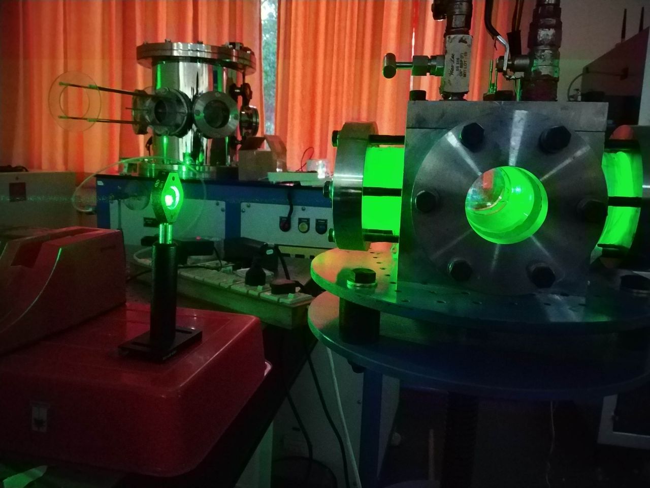
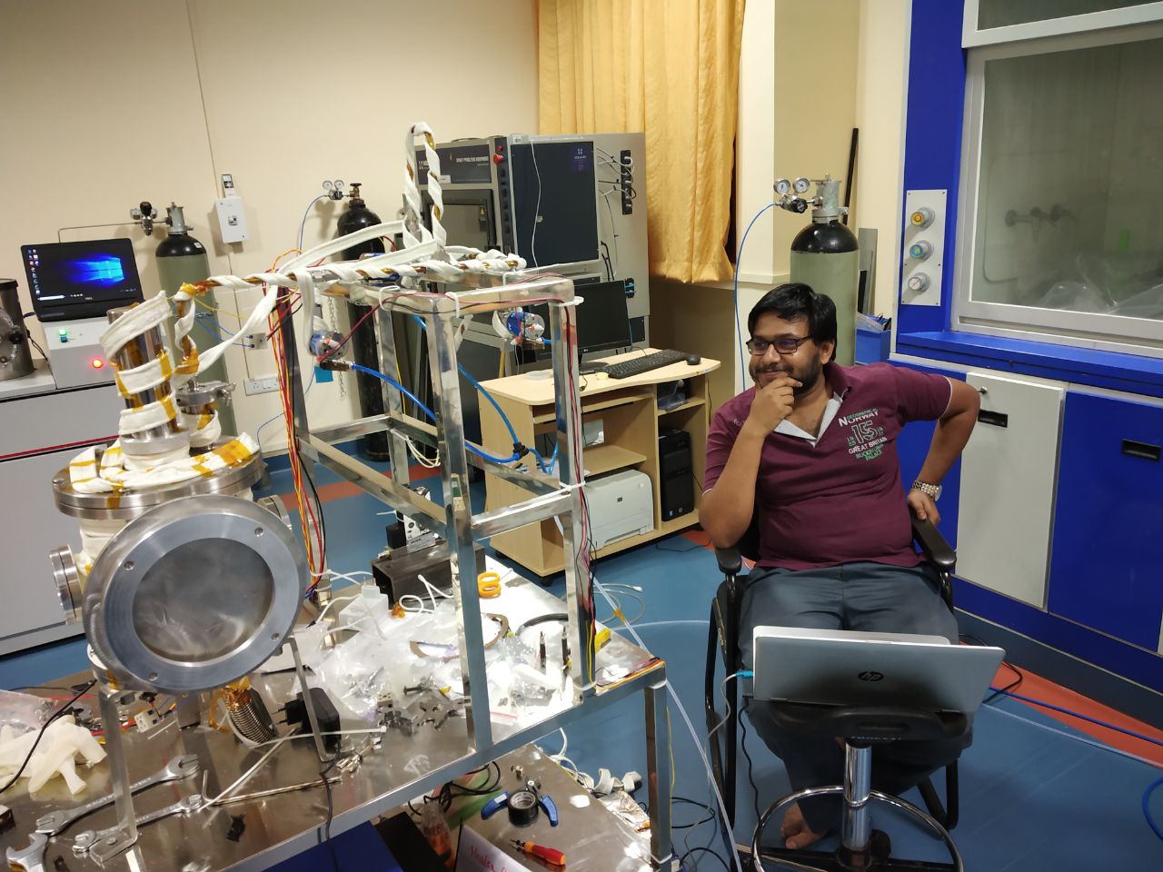
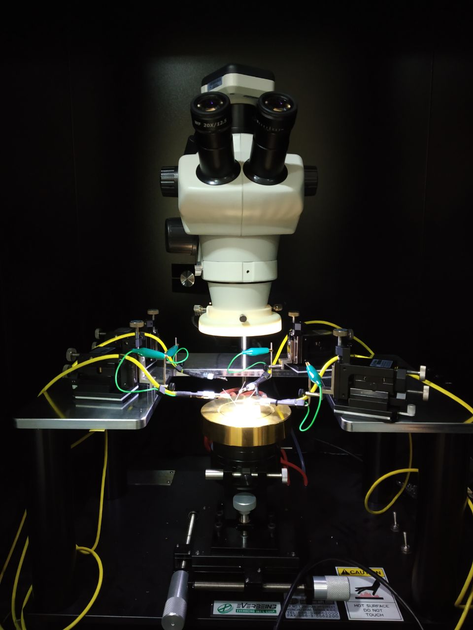
Home-built PLD system Home-built ALD system in progress Thermal ALD System Probe-station
Electronic Materials and Devices (EMERALD) Laboratory
Broadly speaking, our research group focuses mainly on the material and device challenges of the Artificial Intelligence research. Our research interests are on two related technologies: the future Electronic memory devices and Thin film transistors (TFT). In memory options, we are currently studying Resistive Random Access Memory (ReRAM or RRAM) devices and several physical phenomena in this upcoming technology. As the next level, research is ongoing in Neuromorphic memory technology.
In our labs, we study and try to understand the properties of electronic materials apt for these technologies by studying their electronic and opto-electronic properties. For instance, semiconductors with controllable defect levels are useful for the Resistive random access memory (ReRAM) technology. Ultra-thin high-k dielectrics are important for Thin Film Transistor technology. High-mobility semiconductors for TFT's are of great interest to us. We attempt to understand the materials from its molecular electronic structures and to know their charge transport properties in various device configurations. Device performance will shed light on the materials properties as well. The set of materials in our current focus includes 2-dimensional materials including transition metal chalcogenides and graphene derivatives. We employ custom-built Pulsed Laser Deposition (PLD), custom-built Atomic Layer Deposition (ALD), Physical Vapor Deposition techniques and chemical techniques to fabricate thin films of interest. Other important semiconducting materials such as doped ZnO, organic materials and perovskite materials also are of great interest to us. We mostly follow thin film deposition methods that are technology compatible, as per International Technology Roadmaps.
Besides the material characterization techniques, we use Scanning Tunneling Microscope (STM) together with tunneling spectroscopy (STS) to understand the electronic mapping and local density of states (LDOS) of material surfaces. Density functional theory (DFT) calculations are used to understand and predict the results and to modify the materials further for applications. More on the research areas we are focusing is given below.
1. Resistive Random Access Memory (ReRAM) Devices
The aggressive scaling down of the dimensions of the CMOS devices indicates that within this decade, further miniaturization of the memory elements, especially the Flash technology, will meet challenges at various levels due to the direct quantum tunneling of the stored charges and consequent data loss. To circumvent this, various solutions have been proposed and one among them is the suddent changes in the resistance observed in some materials under voltage stress. This phenomenon is interesting for the future memory technology because of its process simplicity (thus, low-cost) and technical compatibility with the existing CMOS technologies. Several materials, e.g. ZnO, TiO2, organic materials, organic-inorganic hybrids, perovskites etc. exhibit reproducible reversible resistance switching. We focus on understanding the mechanisms behind resistive switching in various materials and to explore the scalability issues of ReRAM devices.
Recently, we have developed a technology that enables us unifying the switching parameters of ReRAM devices, by controlling the SET and RESET process via an external bias. Thus, the new technology works with a thin film transistor configuration, where the switching occurs in the channel, which can be controlled by the gate voltage. By this we have better control over the device performance. We demonstarted the viability of this technology employing reduced graphene oxide as the channel (switching) material, and the results has been published recently in Applied Physics Letters (2016).
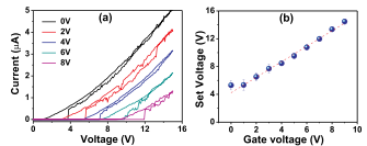
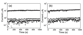
(Left) STM image of rGO, its Local Density of States ; (middle) Gate-bias dependent switching in rGO ReRAM; (right) Endurance measured at different gate voltages.
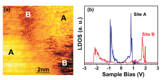
Using Scanning Tunneling Microscope, we probed the influence ofgrain boundaries in ZnO ReRAM devices, and found that grain boundaries behave like degenerate semiconductors. Their distribution in nanometric ReRAM devices would increase the randomness to total randomness, when the deice shrinks to dimensions of the order of 10 nm2. These results were published recently in Nanotechnology (2018).
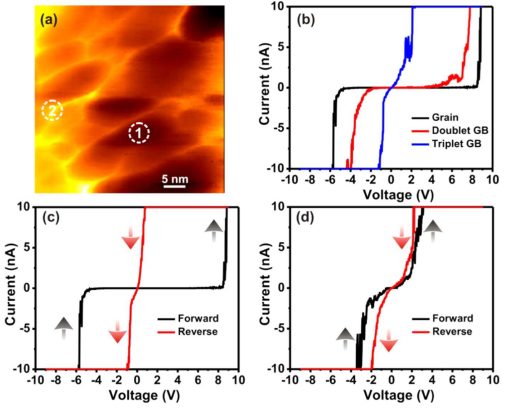
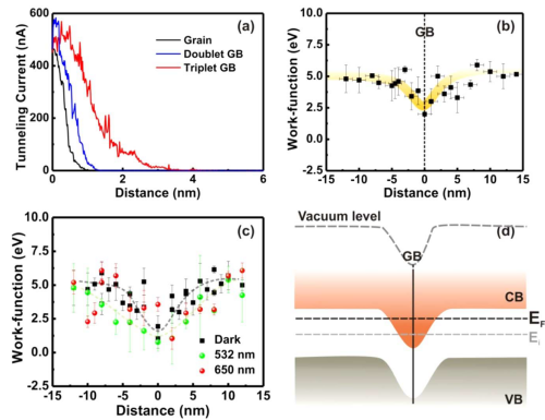
(Left panel): Grain boundaries of ZnO probed by STM and resistive switching on grains and boundaries; (Right panel) Reconstruction of band-diagram of ZnO arounf a doublet grain boundary, using I-z spectroscopy.
Following this, we have been successful in developing graphene based ReRAM devices, with lateral switching capability, and tuneable conductivity employing various surfactant molecules (published in Materials in Electronics (2018)). In addition, we have studied the switching of PMMA thin films and explained the mechanisms in a paper published in Organic Electronics (2016).
2. Thin film transistors (TFT’s)
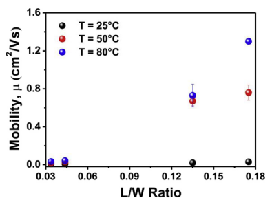
The development of high-mobility materials is the focus of this work. One of our spotlights is 2-dimensional materials, for example, reduced graphene oxide (rGO), derivatives of MoS2, etc., which have defect-induced bandgaps that could be beneficial for the devices. rGO and rGO-based nano-materials systems are under investigation in our group. From the TFT's fabricated using chemically exfoliated graphene, we have achieved a hole mobility of 465 cm2/Vs. We are also studying ZnO, doped with selected doping elements to enhance the channel mobility and to reduce the subthreshold swing as much as possible, within the defect engineering limit of the materials. We employ Scanning Tunneling Microscope (STM) to study the local density of states (LDOS) of the doped semiconductors, their chemical environments and relate it to the carrier transport at nano-scale.
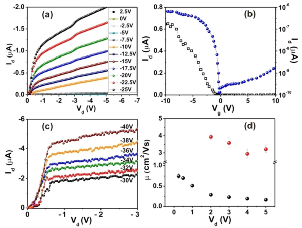
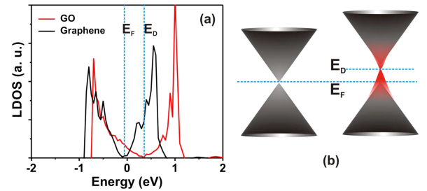
(Left panel) Characteristics of rGO-based 150um and 60 um TFT's. (Right panel) Local Density of States (LDOS) measured using STM at graphene-like and GO-like regions on rGO.
We also demonstrated that liquid-phase exfoliated graphene could be a good alternative for rGO, with much less defects in it. These graphene transistors were exhibiting clear Dirac points with a shift in the Fermi level dur to the electron donating nature of the surfactant molecules used for exfoliation, attached to the edges. These results were published in Material Science and Engineering B recently.
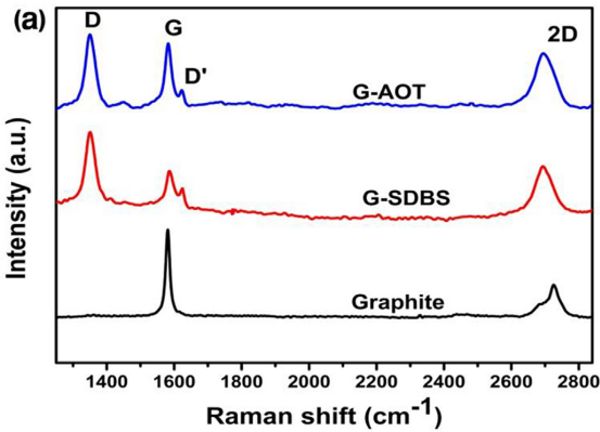
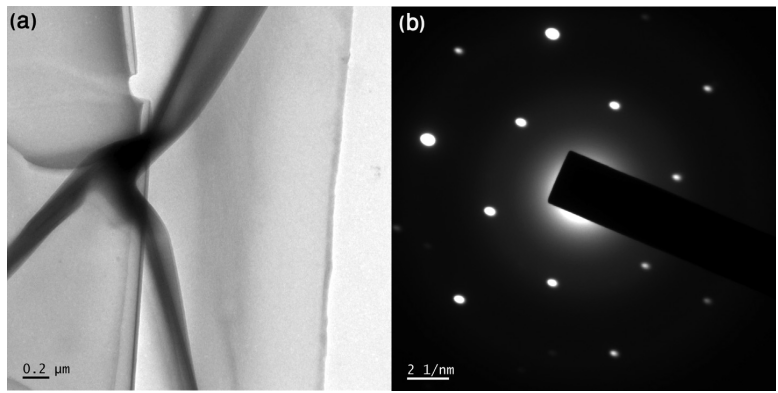
(Left panel) Raman spectra of exfoliated graphene; (middle panel) TEM and SAED patterns of exfoliated graphene layers; (right panel) Ambipolar behavior of graphene TFT's with respect to bias.
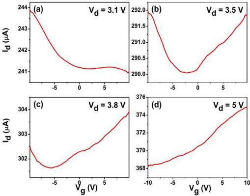
Another work we pursue with is thin film transistors of organic materials. Metal Phthalocyanines are our current materials of interest, since they can be uniformly deposited using thermal evaporation, at low temperature. We recently published a work on CuPc (copper phthalocyanine) transistors in Journal of Science: Advanced Materials and Devices (2018). Works on CoPc and other selected phthalocyanine combinations are progressing in our lab.
(Left panel) Output characteristics of CuPc transistors, with and without post deposition anneal. (Right panel) Influence of the PDA on mobility.
3. Thin film solar cells
The development of solar cells for celestial applications demands high efficiency, low payload, stability for at least 20 years and excellent radiation resistance. There are not many material combinations that can do this work, but the emerging chalcopyrite and stannite materials offer possibilities of developing lower-cost compound solar cells for the satellites.
Development of thin film solar cells has several interesting scientific challenges. The absorber-buffer band alignments and their implications in the cell performance, the interface quality of the p-n junction, inter-layer diffusion mechanisms of elements and their role in the photovoltaic efficiency etc are the major topics of our interest in this category. The grain boundaries of several compound absorber layers are intriguingly influential in photo-electron conversion mechanisms, contrary to their single crystalline counterparts. Grain boundaries of compound semiconductors are one of our main research interests. We employ DFT calculations together with STM to understand various phenomena underlying the higher photoelectron conversion efficiency of polycrystalline semiconducting thin films.
Space Technology Innovations and Characterizations (STIC) Laboratory
The purpose of STIC laboratory is to carry out research and projects related to applications and future missions of ISRO. We are currently carrying out three projects with ISRO Centers:
1. Development of Surface Discharge Sparkplugs (SDS)
Surface discharge sparkplugs have been identified as the next generation sparkplugs, which have already identified its used in aircrafts and racing cars die to high plasma throughput and low power compared to the convensional sparkplugs. Another remarkable thing about semiconductor sparkplug is that the plasma generation does not depend on the pressure of the environment, and thus, the challege posed by Paschen't law can be overcome.
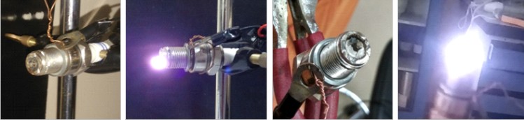
A Memorandum of Understanding (MoU) has been signed between IIST and Liquid Propelsion Systems Center (LPSC, ISRO) for developing a high throughput, low-power sparkplugs for the future cryogenic engines. We have successfully developed a semiconductor sparkplug that operates with DC 1kV power (rather than pulsed 5kV, which creates problems in communication systems in the launch vehicle). The system is under prototype development for the actual space qualification.
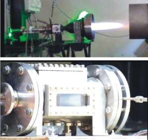
2. Development of Laser Ignition Systems (LIS)
An alternative to the conventional sparkplug that operates at a high voltage is to employ laser-based ignition in space missions. We have signed another MoU with LPSC on developing Laser Ignition Systems (LIS) for future missions. The feasibility of LIS for space applications has been demonstrated by our team at IIST and LPSC.
3. Hard coatings for improving the lifetime of ballbearings in ISRO Spacecrafts.
We have signed an MoU with ISRO Inertail Systems Unit (IISU) for developing surface engineering techniques for improving the life and performance of ball-bearing systems in ISRO Spacecraft mechanisms. This mainly involves the studies on appropriate hard-coatings on ball-bearing systems in spacecrafts, and to study the surface energy modification techniques for improving the wettability of steel ball-bearing systems. For the development of the hard-coatings,we have designed and developed an in-house deposition system, and its optimization is currently in progress.
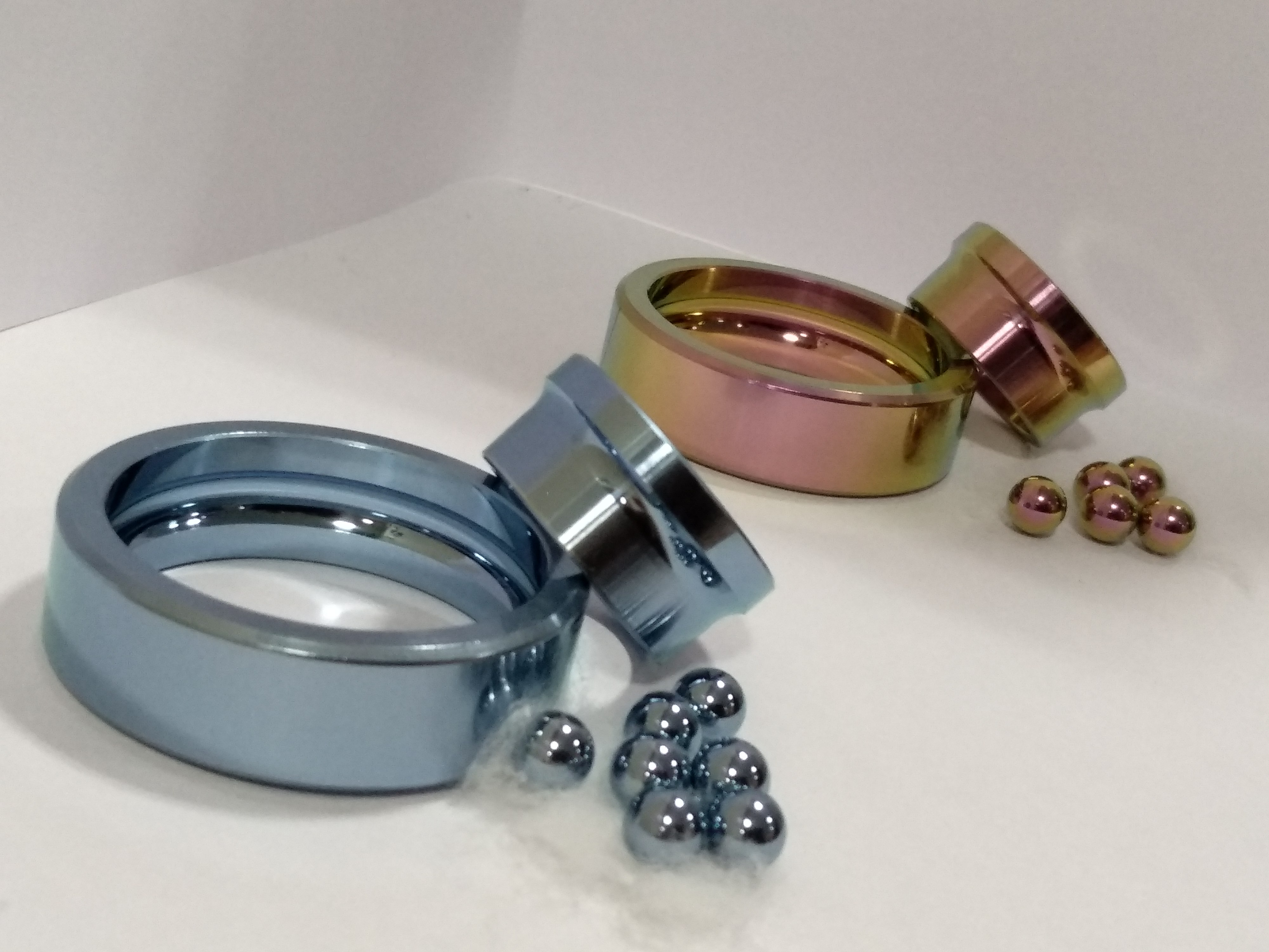
Coatings developed to protect ball bearings from wearing.